8085 is an 8-bit microprocessor as it operates on 8 bits at a time and is created
with N-MOS technology. This microprocessor exhibits some unique characteristics and this is the reason it
still holds popularity among the microprocessors.
Basically, 8085 was the first commercially successful microprocessor by Intel. As some of the architectural drawbacks associated with 8080 were
also eliminated by 8085.
The size of the data bus of 8085 is 8 bits while that of the address
bus is 16. Therefore, can address 64 KB (i.e., 216) memory. Also, as it can perform 8-bit operations thus the size of
ALU is 8-bit.
It also provides operational advantages, as 8085 needs a single +5V
supply with only one clock single of width 320 ns. While 8080 requires
3 power supply lines and 2 clock signals of 500 ns.
Bit:
A bit is a single binary digit.
Word:
A word refers to the basic data size or bit size that can be
processed by the arithmetic and logic unit of the processor. A
16-bit binary number is called a word in a 16-bit processor.
Memory Word: The number of bits that can be stored in a register or memory
element is called a memory word.
Bus:
A bus is a group of wires (lines) that carry similar
information.
System Bus: A system bus is a group of wires used for communication between
the microprocessor and peripherals.
Address Bus: It carries the address, which is a unique binary pattern used
to identify a memory location or an I/O port.
Data Bus: The data bus is used to transfer data between memory and
processor or between I/O device and processor.
Control Bus: The control bus carries control signals, which consist of
signals for selection of memory or I/O device from the given
address, direction of data transfer, and synchronization of data
transfer in case of slow devices.
Internal Architecture of 8085 Microprocessor:
The architecture of the 8085 microprocessor provides an idea about
what are the operations to be executed and how these are
performed.
It can perform operations that are given below:
-
Operates on and stores 8-bit data.
-
It executes arithmetic and logic operations.
-
8085 also sequences the instructions to be executed.
-
Stores data temporarily.
However, to perform all such operations, the processor needs a
control unit, arithmetic logic unit, registers, buses,, etc.
We have already discussed how CU, ALU,, and buses function in a
microprocessor. Here, in this article, we will discuss the detailed
architecture of the 8085 microprocessor and how it operates.
The figure below represents the architectural representation of
the 8085 microprocessor:
Functional Units of 8085:
1. Registers: These are nothing but a set of flip flops. These
are basically used to hold (store) the data general-purpose pose registers– 8085 microprocessors contain
general-purpose registers that are present inside the
microprocessor stories 8-bit dtor to execute a program.
The general-purpose pose registers are B, C, D,E, H and L. These
registers can be combined to form pairs – BC, DE andtor to execute the
16-bit operation.
These are programmable registewhichthat means these registers are
accessed by the programmer to insert and transfer the data by making
use of instructions.
Temporary registers: These registers are used by the ALU to store the
data temporarily and these are not accessed by the programmer.
These are of 2 types:
-
Temporary data register
– It is an 8-bit register that holds the operand and provides it
to the ALU for program execution. Also, the immediate results
are stored by the ALU in these registers.
-
-
W and Z register
– These registers are also used to hold the temporary values. It
is used by the control section of the microprocessortoo store
the data during operations.
-
Program Counter (PC): This16-bitt register deals with sequencing the execution
ofthe instruction. The microprocessor uses this register
to sequence the execution of the instructions. The function of
the program counter is to point to the memory address from which
the next byte is to be fetched.
-
-
Stack Pointer (SP): The stack pointer is also a 16-bit register used as a
memory pointer. It points to a memory location in read-write
memory, called the stack.
-
-
Instruction Register/Decoder: Temporary store for the current instructions of a
program. Latest instruction sent here from memorybeforeo
execution.The decoderr then takes instruction and decodes or
interprets the instruction. Decoded instruction then passed
tothe
next stage.
-
-
Memory Address Register: Holds address, received from PC of next program
instruction.
-
-
Control Generator: It generates a signal within μP to carry out the
instructions which have been decoded.
-
-
Register Selector: This block controls the use of the register stack.
-
-
General Purpose Registers: μP requires extra registers for versatility. It can be used to
store additional data during a program.
What is 8085 Microprocessor?
-
It hasan 8 bit data bus and 16 bit address bus,
thus it is capable of addressing 64 KB of memory.
-
It has 8 bit ALU 8 bit ALU that can perform 8 bit
operations.
-
Lower order address bus is multiplexed with data bus to
minimize the chip size.
-
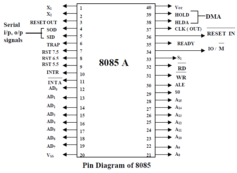
The 8085 microprocessor is an 8-bit processor available
as a 40-pin IC package (shown the figure below) and uses
+5 V for power. It can run at a maximum frequency of 3
MHz.
-
-
-
The 8085 has extensions to support new interrupts, with
three maskable interrupts (RST 7.5, RST 6.5 and RST 5.5),
one non-maskable interrupt (TRAP), and one externally
serviced interrupt (INTR).
-
-
Three control signals are available on chip:
(i) RD : it is a active low signal. Which indicate that
the selected IO or Memory device is to be read and data
is available on the data bus. (ii) WR : it is a active
low signal which indicate that the data on the data bus
are to be written into a selected memory or IO location.
(iii) ALE : it is a +ve going pulse generated every time
the 8085 begins an operation (machine cycle), which
indicate that the bits on AD7-AD0 are address
bits.
-
-
Three status signals are available on chip:
(i) IO/M : this is a status signal used to differentiate
between IO and Memory operations. If it is high then IO
operation and If it is low then Memory operation. (ii)
S1 and S0 : status signals similar to IO/M, can identify
various operations that are rarely used in the
systems.
Internal Architecture of 8085 Microprocessor:
The architecture of 8085 consists of three main sections,
ALU (Arithmetic and Logical Unit), timing and control unit
and Registers (shown in the following figure).

Arithmetic and Logic Unit (ALU): The ALU performs the actual numerical and logical
operations.
Timing & Control Unit: It generates timing and control signals, which are
necessary for the execution of instructions.
-
It controls data flow between CPU and peripherals
(including memory).
-
It provides status, control and timing signals, which are
required for the operation of memory and I/O
devices.
-
8085 System Bus: Microprocessor communicates with memory and other
devices (input and output) using three buses: Address Bus,
Data Bus and Control Bus.
-
Address Bus: The Address bus consists of 16 wires. The size of
the address bus determines the size of memory, which can
be used. To communicate with memory the microprocessor
sends an address on the address bus to the memory. Address
bus is unidirectional, i.e., numbers only sent from microprocessor to memory.
-
Data Bus: Bus is bidirectional. Size of the data bus
determines what arithmetic can be done. Data bus also
carries instructions from memory to the
microprocessor.
-
Memory size = 2A x D where, A denotes the address lines, and D
denotes the data lines.
-
Control Bus: Control bus are various lines which have specific
functions for coordinating and controlling μP operations.
The control bus carries control signals partly
unidirectional, partly bidirectional. Control signals are
things like reading or writing.
Registers: 8085 has six general-purpose registers to store 8-bit
data, these are identified as B, C, D, E, H, and L. They can
be combined as register pairs BC, DE, and HL to perform some
16-bit operations.
-
Accumulator: The accumulator is an 8-bit register included as a
part of the Arithmetic Logic Unit (ALU). This register is
used to store 8-bit data and to perform arithmetic and
logical operations. The result of an operation is stored
in the accumulator.
-
Flag Register: The ALU includes five flip-flops. They are called
Zero (Z), Carry (CY), Sign (S), Parity (P), and Auxiliary
Carry (AC) flags. The microprocessor uses these flags to
test data conditions. The conditions (set or reset) of the
flags are tested through the software instructions. The
combination of the flag register and the accumulator is
called Program Status Word (PSW) and PSW is the 16-bit
unit for stack operation.

-
-
Program Counter (PC): This 16-bit register deals with sequencing the
execution of an instruction. The microprocessor uses this
register to sequence the execution of the instructions.
The function of the program counter is to point to the
memory address from which the next byte is to be
fetched.
-
Stack Pointer (SP): The stack pointer is also a 16-bit register used as
a memory pointer. It points to a memory location in
read-write memory, called the stack.
-
Instruction Register/Decoder: Temporary store for the current instructions of a
program. Latest instruction sent here from memory prior to
execution. The decoder then takes instruction and decodes
or interprets the instruction. Decoded instruction then
passed to the next stage.
-
Memory Address Register: Holds address, received from PC of next program
instruction.
-
Control Generator: It generates a signal within μP to carry out the
instructions which have been decoded.
-
Register Selector: This block controls the use of the register
stack.
-
General Purpose Registers: μP requires extra registers for versatility. It can be
used to store additional data during a program.
Operations of Microprocessor:
The microprocessor performs the following four operations
using address bus, data bus, and control bus:
-
Memory Read: Reads data (or instruction) from
memory.
-
Memory Write: Writes data (or instruction) into
memory.
-
I/O Read: Accepts data from the input device.
-
I/O Write: Sends data to the output device.
An instruction is a command to the microprocessor to
perform a given task on a specified data. Each instruction
has two parts, one is task to be performed, called the
operation code (opcode), and the second is the data to be
operated on called the operand. The 8085 instruction set is
classified according to word size.
-
One-Byte Instructions: A 1-byte instruction includes the opcode and
operand in the same byte. Operands are internal registers
and are coded into the instruction.
-
Two-Byte Instructions: In a two-byte instruction, the first byte specifies
the operation code and the second byte specifies the
operand. Source operand is a data byte immediately
following the opcode.
-
Three-Byte Instructions: In a three byte instruction, the first byte
specifies the opcode and the following two bytes specify
the 16-bit address. Note that, the second byte is the
low-order address and the third byte is the high-order
address.
The 8085 Addressing Modes:
The various formats for specifying operands are called
the addressing modes. For 8085, they are
-
Immediate Addressing:
-
Data is provided in the instruction.
-
Load the immediate data to the destination
provided.
-
Example: MVI A, 12 H
-
-
Register Addressing:
-
Data is provided through the registers.
-
Example: MOV B, C
-
-
Direct Addressing:
-
Used to accept data from outside devices to store
in the accumulator or send the data stored in the
accumulator to the outside device.
Applications of 8085 microprocessor:
8085 finds its major applications in programmable
calculators as well as in numerical control and
environmental monitoring systems. These are also
used in switching, banking, and financial
systems.
-
Example: MOV A, [1000]
-
-
Indirect Addressing:
-
The effective address is calculated by the
processor and the contents of the address is used to
form a second address. The second address is where
the data is stored.
-
Example: MOV A, [[1000]]
-
-
Implicit addressing:
-
In this addressing mode the data itself specifies the
data to be operated upon.
-
Example: CMA ; Complement the contents of
accumulator
8085 Instruction Set:
An instruction is a binary pattern designed inside a
microprocessor to perform a specific function. Each
instruction is represented by 8 bit binary value.
Instruction set can be categorised int0 5 types:

-
Data transfer instructions:
-
These instructions are used to transfer data from
one register to another register, from memory to
register or register to memory.
-
When an instruction of data transfer group is
executed, data is transferred from the source to
the destination without altering the contents of
the source.
-
Examples: MOV, MVI, LXI, LDA, STA, etc.
-
-
Arithmetic instructions:
-
These instructions are used to perform arithmetic
operations such as addition, subtraction,
increment or decrement of the content of a
register or memory.
-
Examples: ADD, ADC, ADI, DAD, SUB, INR, DCR,
etc.
-
-
Logical instructions:
-
These instructions are used to perform logical
operations such as AND, OR, compare, rotate
etc.
-
Examples: ANA, ANI, ORA, ORI, XRA, CMA, CMC ,
STC, CMP, RLC, RAL, RAR, etc.
-
-
Branching Instructions:
-
These instructions are used to perform
conditional and unconditional jump, subroutine
call and return, and restart.
-
Examples: JZ, JNZ, JC, JNC, JP, JM, JPE, JPO,
CALL, RET, RST, etc.
-
-
Machine Control Instructions:
-
These instructions control machine functions such
as Halt, Interrupt, or do nothing.
-
The microprocessor operations related to data
manipulation can be summarized in four functions:
copying data, performing arithmetic operations,
performing logical operations, testing for a given
condition and alerting the program sequence.
-
Example: PUSH, POP, HLT, XTHL, NOP, EI, DI,
etc.
Applications of 8085 microprocessor:
8085 finds its major applications in programmable
calculators as well as in numerical control and
environmental monitoring systems. These are also used
in switching, banking and financial systems.


Post a Comment
Ask any Doubt related to this site...